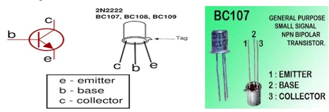
To plot the transistor (BJT) characteristics of CE configuration.
| S.No. | Name | Range | Quantity |
| 1 | R.P.S | (0-30)V | 2 |
| 2 | Ammeter | (0-30)mA MC, (0-250)μA MC | 1, 1 |
| 3 | Voltmeter | (0-30)V MC, (0-1)V MC | 1, 1 |
| S.No. | Name | Range | Quantity |
| 1 | Transistor | BC 107 | 1 |
| 2 | Resistor | 10KΩ, 1KΩ | 1, 1 |
| 3 | Bread Board | - | 1 |
| 4 | Wires |
A BJT is a three terminal two - junction semiconductor device in which the conduction is due to both the charge carrier. Hence it is a bipolar device. BJT is classified into two types - NPN & PNP. A NPN transistor consists of two N types in between which a layer of P is sandwiched. The transistor consists of three terminal emitter, collector and base. The emitter layer is the source of the charge carriers and it is heavily doped with a moderate cross sectional area. The collector collects the charge carries and hence moderate doping and large cross sectional area. The base region acts a path for the movement of the charge carriers. In order to reduce the recombination of holes and electrons the base region is lightly doped and is of hollow cross sectional area. Normally the transistor operates with the EB (emitter-base) junction forward biased.
Input Characteristics

Specification: BC107/50V/0.1A,0.3W,300 MH
Input Characteristics

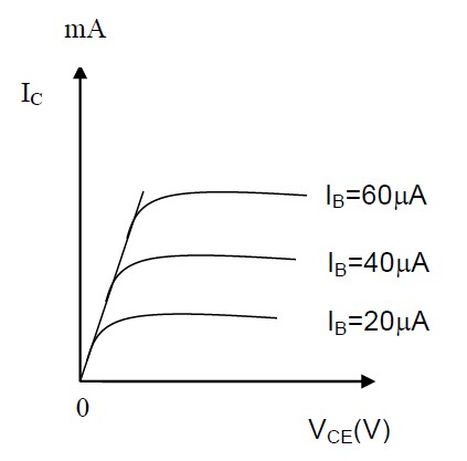
Output Characteristics

Input Characteristics
| V CE= 0 V | V CE=2V |
| VBE (V) IB(μA) | VBE (V) IB(μA) |
Output Characteristics
| VB=20μA | VB=40μA |


Get all latest content delivered to your email a few times a month.
Resources: